Diode reverse recovery characteristics are a key factor to consider when designing power electronics systems. Reverse recovery is the process by which a diode, when switched off, returns to its forward-biased state. This process, however, is not instantaneous, and the diode’s reverse-recovery characteristics determine how long this process takes.
When a diode is switched off, the junction capacitance has to be discharged. This is what determines the device’s reverse recovery time. Reverse recovery time is usually specified as the time it takes for the current to drop from its peak reverse current to a certain specified level.
Diode reverse recovery characteristics are important for power electronics systems, as the reverse recovery time of a diode affects the power dissipation of the system. If the diode’s reverse recovery time is too long, the power dissipation of the system increases, and the system’s efficiency suffers.
To reduce power dissipation, designers must choose diodes with good reverse recovery characteristics. To achieve this, designers must be familiar with the diode’s reverse recovery time, reverse recovery charge, and reverse recovery current.
It is also important to note that diodes with a lower reverse recovery time can suffer from increased forward voltage drop. Additionally, diodes with a shorter reverse recovery time can cause ringing in the power system due to the resonance of the junction capacitance.
Reverse recovery characteristics of a power diode refer to the behavior of the diode when it switches from forward conduction to reverse blocking mode. During forward conduction, the diode allows current to flow in the forward direction with a low forward voltage drop. However, when the polarity of the applied voltage is reversed, the diode should block current flow in the reverse direction.
In reality, there is a finite time delay for the diode to transition from forward conduction to reverse blocking mode. This time delay is called the reverse recovery time (t_rr) and is an important parameter for power diodes, especially in high-frequency applications.
During the reverse recovery time, the diode conducts a small amount of reverse current due to the stored charge in the diode depletion region. This reverse current is known as the reverse recovery current (I_rr) and can cause voltage spikes and switching losses in the circuit.
The reverse recovery characteristics of a power diode can be measured using a test circuit that applies a forward current to the diode and then switches the current to a reverse direction. The time taken for the diode to switch from forward conduction to reverse blocking mode, and the magnitude of the reverse recovery current, can be measured and analyzed to determine the diode's performance in a given application.
Diode reverse Recovery Characteristics
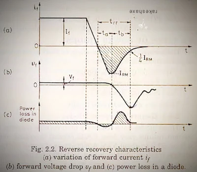
After the forward diode current decays to zero, the diode continues to conduct in the rear direction because of the presence of stored charges in the two layers. The rear current overflows for a time called rear recovery time trr.
The diode regains its blocking capability until rear recovery current decays to zero. The reverse recovery time trr, is defined as the time between the instant forward diode current becomes zero and the instant reverse recovery current decays to 25% of its reverse peak value IRM.
The reverse recovery time is composed of two segments of time ta, and tb, ie., trr=ta+tb . Time ta, is the time between zero erossing of forward current and peak reverse current IRM During the time ta, charge stored in depletion region is removed. Time tb is measured from the instant of IRM to the instant where 0.25 IRM is reached, During fa, charge from the two semiconductor layers is removed. The shaded area in Fig. 2.2 (a)
represents the stored charge, or reverse recovery charge, QR which must be removed during the reverse recovery time trr. The ratio tb/ta, is called the softness factor or S-factor.
This factor is a measure of the voltage transients that do during the time diode recovers. Its usual value is concinnity and this indicates low oscillatory rear recovery process. In case S- factor is small, diode has large oscillatory over voltages.
A diode with S-factor equal to one is called soft-recovery diode and a diode with S-factor less than one is called snappy-recovery diode or fast-recover diode.
peak inverse current=IRM=ta.di/dt .....eq(1)
where di/dt=the rate of change reverse current.
stored charge or reverse recovery charge=QR=0.5.IRM.trr
or IRM=2QR(1/trr) ......(2)
If trr≅ta,then from eqn(1)
IRM=trr.di/dt .......(3)
From eqn(2) and (3) , we get
trr.di/dt=2QR(1/trr)
or trr=[2QR(di/dt)(-1)]o.5 ......(4)
From eqn(1) ,with ta≅trr , we get
IRR=trr.di/dt
or IRR=[2QR(di/dt)]0.2 .......(5)
It is seen from Eqs. (2.4) and (2.5) that reverse recovery time and peak inverse current are dependent on storage charge and rate of change of current di/dt.
The storage charge depends upon the forward diode current IF.
This shows that reverse recovery time and peak inverse current depend on forward field current.
A power-electronics engineer must know peak reverse current, stored charge, S-factor, PIV etc in order to be able to design the circuitry employing power diodes.
These parameters are generally specified in the roster supplied by the diode manufacturers.
Summary
it is important to consider the reverse recovery characteristics of a diode when designing a power electronics system. By selecting diodes with good reverse recovery characteristics, designers can ensure that their systems are efficient and reliable.

Comments